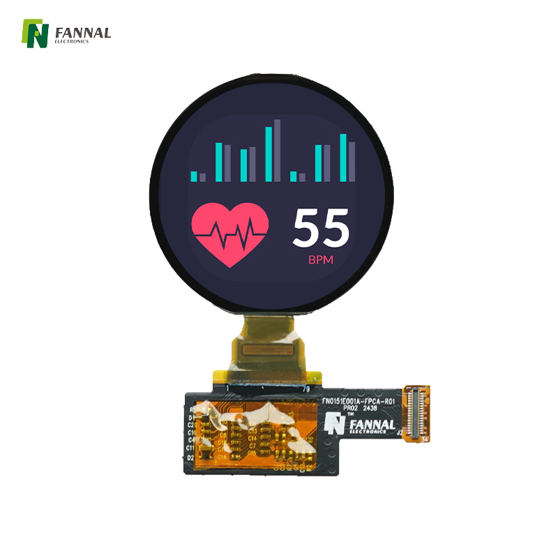

High Resolution: With its pixel density, the display ensures crisp and clear visuals, making it suitable for detailed graphics and user interfaces.
Compact Design: The round shape and small size make it an excellent choice for smartwatches, fitness trackers, and other portable gadgets.
Low Power Consumption: The OLED technology allows for power-efficient operation, extending battery life in wearable devices.
This display panel is an excellent solution for developers looking to create engaging and visually appealing wearable applications.
|
LCD size(inch): |
1.504 (Diagonal) |
|
Resolution: |
466(H)×466(V) |
|
Pixel Pitch: |
81.99(H)x81.99(V) |
|
Active Area(mm): |
38.207(H)×38.207(V) |
|
Module Size(mm): |
40.71×40.81×0.82 |
|
Display type: |
AMOLED |
|
Interface: |
MIPI&SPI |
|
View Direction: |
ALL |
| Power Supply: | 3.3 |
| Luminance(cd/m2): |
600(Typ.) |
Interface:
|
Pin No. |
Symbol |
I/O |
Description |
| 1 | MTP_PWR | P | OTP Panel. |
| 2 |
GND |
P |
Ground. |
| 3 | D0P | I |
MIPI DSI Positive differential data signal. |
| 4 | D0N | I | MIPI DSI Negative differential data signal. |
|
5 |
GND |
P |
Ground. |
| 6 | CLKP | I | MIPI DSI Positive differential data signal. |
| 7 | CLKN | I | MIPI DSI Negative differential data signal. |
| 8 | GND | P | Ground. |
| 9 |
D1P |
I |
MIPI DSI Positive differential data signal. |
| 10 |
D1N |
I |
MIPI DSI Negative differential data signal. |
| 11 | GND | P | Ground. |
| 12 | IM0 | I/O | Interface type selection. |
| 13 | IM1 | I/O | Interface type selection. |
| 14 | GND | P | Ground. |
| 15 | NC | - | No connection. |
| 16 | GND | P | Ground. |
| 17 | D1 | I | Serial input signal in SPl l/F. The data is input
on the rising edge of the SCL signal. lf not used, please connect to VSSlO. |
| 18 | D0 | I |
Serial input signal in SPl l/F. The data is input on the rising edge of the SCL signal. lf not used, please connect to VSSlO. |
| 19 | GND | P | Ground. |
| 20 | CSB | I | Chip select input pin in SPI I/F. If not used, please connect to VDDIO. |
| 21 | SCL | I | Pixel clock input signal. |
| 22 | SDI | I | Serial data input signal. |
| 23 | SDO | I | Serial data output signal. |
| 24 | RESET | I | Reset signal input. |
| 25 | TE | O | Tearing effect output pin to synchronize
MCU to frame writing, activated by S/W command. When this pin is not activated, this pin is output low. |
| 26 | OLED_EN | O | Power IC enable control pin(Note:"H"=VDD level, "L"=VSSI level. |
| 27 | SWIRE | O | Swire protocol setting pin of Power IC. |
| 28 | NC | - | No connection. |
| 29 | VCI | P | Supply analog voltage. |
| 30 | VDDIO | P | Power supply for display driver IC interface and logic system. |
| 31 | GND | P | Ground. |
| 32 | ELVDD | P | Positive Power supply for Panel. |
| 33 | GND | P | Ground. |
| 34 | ELVSS_IN | P | Negative Power supply for Panel. |
Electrical Characteristics:
|
Parameter |
Symbol: |
Min. |
Max. |
Unit |
|
Supply Voltage |
VDDA |
-0.3 |
5.5 |
V |
| Supply voltage | VDDIO | -0.3 | 5.5 | V |
